In the ever-evolving landscape of technology, the integrated circuit board (PCB) has emerged as a cornerstone of modern innovation. This intricate assembly of conductive patterns and electronic components has become the silent hero, powering a myriad of devices from smartphones to spacecraft. As we delve into the intricate world of PCB manufacturing, we uncover a journey marked by relentless innovation, sustainability efforts, and the profound impact on various industries. Join us as we explore the challenges and future prospects of the PCB factory, a place where complexity meets precision.
The Heart of Modern Electronics: The Integrated Circuit Board Factory
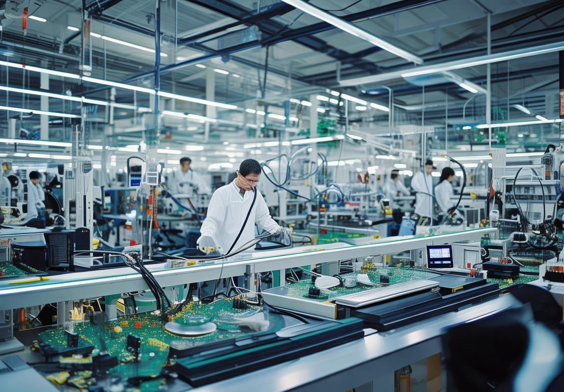
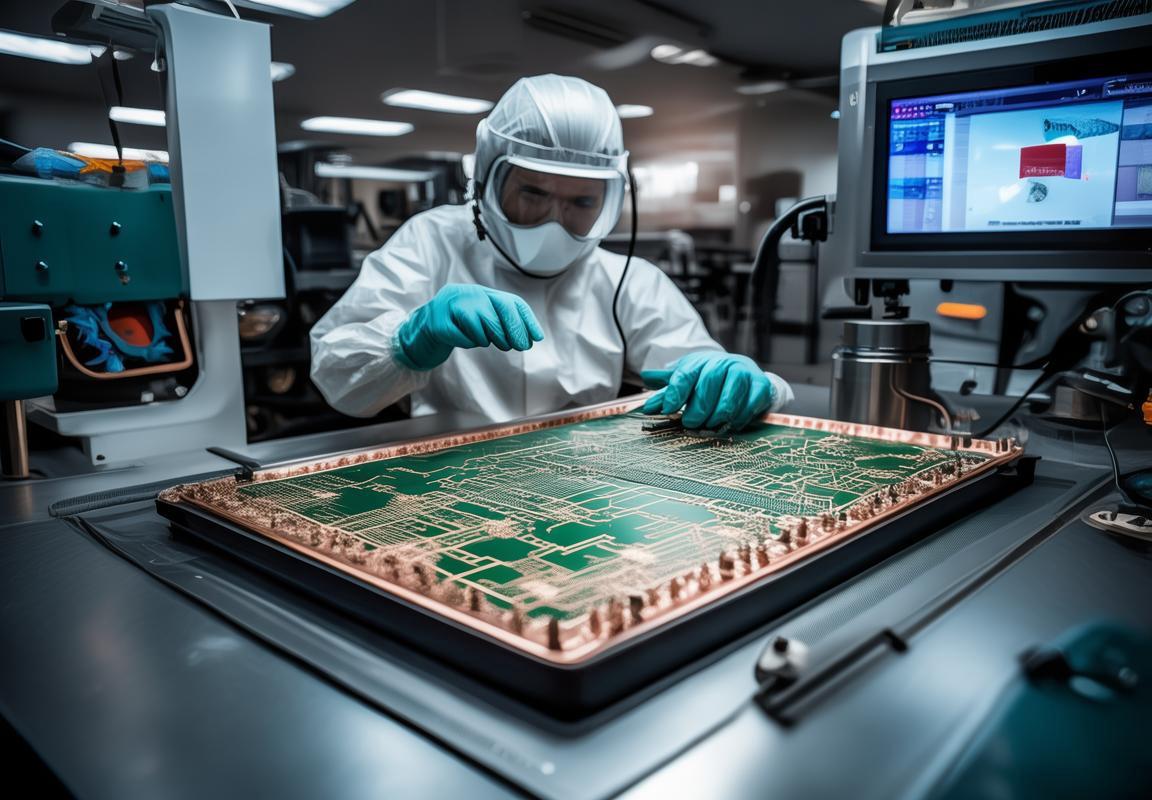
The Integrated Circuit Board (ICB) factory stands as the beating heart of modern electronics. It’s a place where raw materials are transformed into intricate pieces of technology that power everything from smartphones to medical devices. Picture this: rows upon rows of automated machinery, engineers in white coats, and a hum of activity that speaks of precision and innovation.
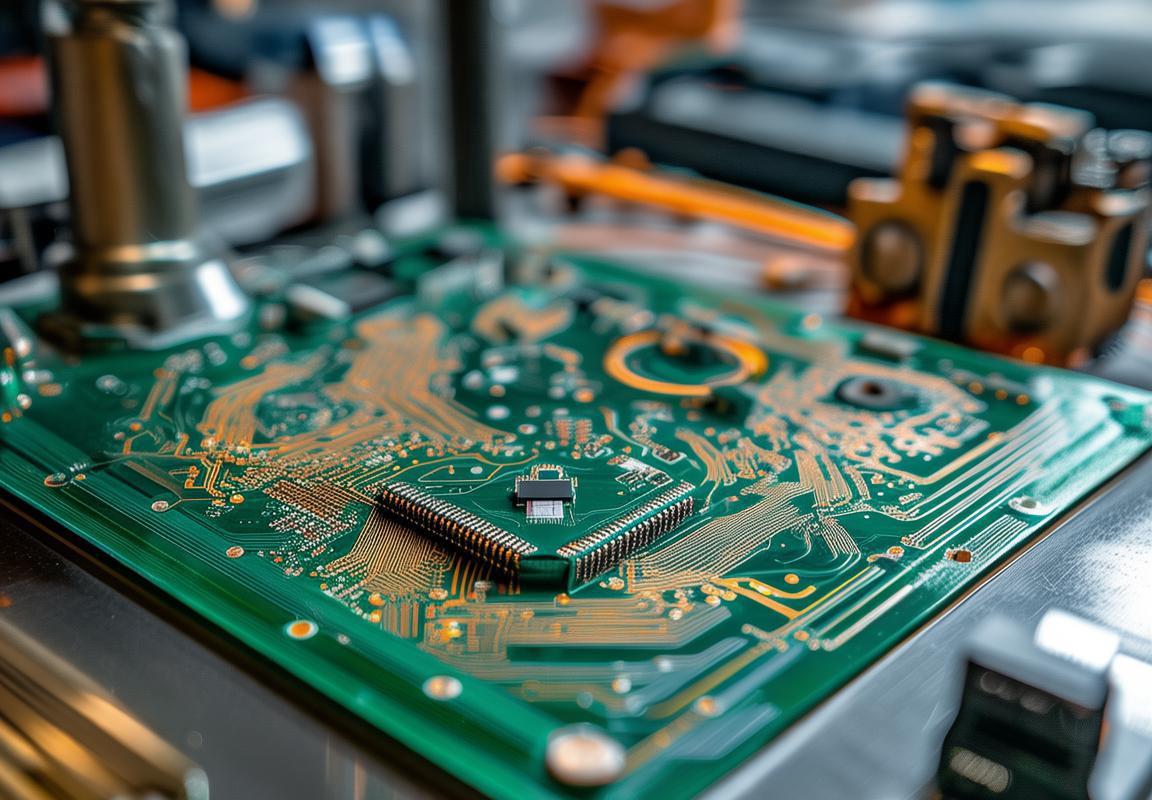
At the heart of the factory, you’ll find a sea of interconnected machines, each with a specific task to perform. The journey begins with a sheet of copper-clad laminate, a material that’s the foundation of every PCB. It’s a delicate balance of copper and non-conductive materials that makes the PCB both conductive and durable.
As the sheet moves through the factory, it’s first etched to create the pathways for the electrical connections. The precision required for this step is almost surgical, with chemical baths carefully removing the unwanted material. It’s a process that requires not just skill but also a keen eye for detail.
Next, the etched copper is covered with a layer of solder mask. This protective layer not only ensures that the copper traces don’t short-circuit but also provides a surface for the silk screen printing. The silk screen is where the PCB’s identification and connection points are marked, guiding the placement of components later on.
After the silk screen process, the board is sent through a series of drills. These holes are crucial for connecting components to the copper traces. The drills are so precise that they can create holes that are only a few micrometers in diameter, a testament to the advanced technology at work.
With the holes drilled, the PCB moves on to the component placement area. Here, automated pick-and-place machines work with incredible speed and accuracy, placing resistors, capacitors, and other electronic components onto the board. The process is repeated until each component is in its designated spot.
Once the components are in place, the PCB enters the reflow oven. Here, the board is heated to temperatures that melt the solder, which then flows into the joints between the components and the copper traces. The board is carefully cooled to solidify the solder, creating a permanent connection.
The next step is the testing phase. The PCB is subjected to a series of electrical tests to ensure that the connections are sound and that the board operates as intended. Any defects are noted and corrected, often by a skilled technician who can identify issues that automated systems might miss.
After testing, the PCB might undergo additional processes like hole plating, which fills the drilled holes with copper to improve the electrical conductivity, or surface finishing, which provides corrosion resistance and improves the solderability of the board.
The final stages of the process involve packaging and quality assurance. Each PCB is carefully wrapped to protect it during shipping, and it’s then quality-checked one last time to ensure that it meets the stringent standards required by the electronics industry.
Throughout this journey, the ICB factory is a hub of activity and precision. Engineers monitor the machines, ensuring they run smoothly and efficiently. Technicians troubleshoot any issues that arise, and quality control teams meticulously inspect every board to ensure it’s free of defects.
The ICB factory is not just a place of production; it’s a place of continuous innovation. New materials, technologies, and methodologies are constantly being developed to improve the efficiency and quality of PCBs. From the smallest consumer gadget to the most sophisticated aerospace technology, the PCB factory is the unsung hero of the electronics world, quietly manufacturing the building blocks of modern society.
Inside the World of PCB Manufacturing
Navigating the halls of a modern integrated circuit board (PCB) factory is akin to stepping into a bustling city of technology. The air is filled with the hum of machinery and the faint whiff of chemicals, a testament to the intricate processes that turn raw materials into the backbone of countless electronic devices.
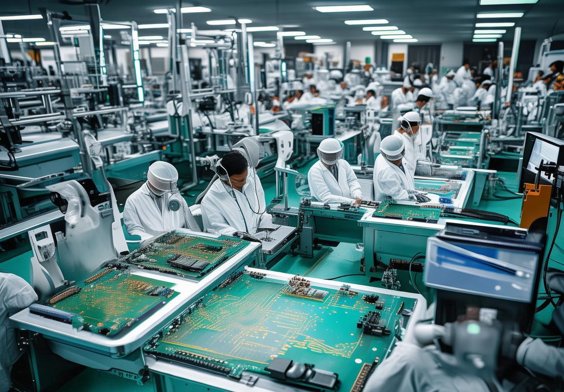
The heart of the factory lies in the cleanrooms, where the magic happens. These sterile environments are meticulously controlled for temperature and humidity to prevent any contaminants from spoiling the delicate circuits. Workers, clad in white suits and hoods, move with practiced grace, their every action contributing to the creation of a tiny, intricate world.
Inspecting the floor, you’ll notice rows upon rows of machinery, each performing a specific task in the PCB manufacturing process. There are etching baths, where the copper patterns are transferred onto the non-conductive substrate, and chemical vats that wash away the unneeded material. The precision required is astonishing; even a tiny speck of dust can render a board unusable.
As you wander through the factory, you might come across a machine that lays down the copper foil. This process, known as lamination, involves applying a layer of copper onto the insulating material. It’s a delicate balance of heat and pressure to ensure that the copper adheres properly without damaging the substrate.
Once the copper layer is in place, the boards move on to the photolithography station. Here, a photographic process is used to transfer the intricate circuit patterns onto the copper surface. The workers carefully align the masks, which are essentially stencils with the circuit designs, and then expose the boards to light-sensitive chemicals.
After the exposed areas are developed, the unneeded copper is etched away, leaving behind the desired circuit patterns. This step is crucial for the functionality of the board and requires a precise chemical mixture and timing to achieve the desired depth and clarity of the tracks.
The boards then move through a series of cleaning stations, where they are bathed in various solvents to remove any remaining contaminants or photoresist. The cleanliness of these boards is paramount, as any foreign particles can cause shorts or disrupt the flow of electricity.
In some factories, the boards are now ready for the drilling phase. A machine equipped with precision drills carefully pokes thousands of holes through the board, each one meticulously placed to accommodate the tiny components that will soon be soldered into place. The drills spin at incredible speeds, yet the factory’s advanced control systems ensure that the holes are perfectly round and at the correct depth.
The next stop is the soldermask application, where a protective layer is applied to prevent solder from adhering to unintended parts of the board. This process is often automated, with machines that spray or roll the soldermask onto the board, then cure it with heat or UV light.
With the protective layer in place, the boards are now ready for the component placement. This can be a manual process, where skilled workers place each component by hand, or it can be highly automated, with robots that place hundreds of components in seconds. The accuracy and consistency are incredible, a testament to the precision engineering of the machinery.
Once all components are in place, the boards are sent through a reflow oven. Here, the components are soldered into place with a precise temperature and time profile. It’s a delicate dance of heat and cooling to ensure that the solder joints are strong and reliable.
After cooling, the boards are tested to ensure that all components are functioning correctly and that there are no shorts or opens in the circuitry. This is done through a variety of tests, including functional testing and electrical testing, which can include everything from simple continuity checks to complex simulations of real-world use.
Finally, the boards are inspected visually for any defects, such as smudges, burn marks, or incorrectly placed components. A team of quality control engineers meticulously examines each board, ensuring that it meets the stringent standards required for high-quality PCBs.
The journey through the PCB manufacturing process is a marvel of engineering and precision. It’s a process that combines the art of manual craftsmanship with the power of cutting-edge technology to produce the intricate, high-performance circuits that power our modern world. Each step is crucial, and each machine plays a vital role in the final product, a product that is often taken for granted but is the lifeblood of our interconnected society.
The Journey of a PCB: From Raw Materials to Final Product
In the intricate world of electronics, the Printed Circuit Board (PCB) is the unsung hero, the backbone of every electronic device. The journey of a PCB from raw materials to the final product is a testament to the precision and innovation that drives modern manufacturing.
The process begins with a selection of high-quality materials. Copper, a conductive metal, is chosen for its excellent electrical properties. It’s rolled into thin sheets, typically around 1.6 millimeters thick, which will form the pathways on the PCB. These sheets are then coated with a layer of insulating material, usually a fiberglass-reinforced epoxy, to prevent short circuits.
Next, the copper sheets are chemically etched to create the intricate patterns that define the PCB’s circuitry. This process involves dipping the sheets into an acid bath, where the exposed copper reacts and is dissolved away, leaving behind the desired circuit paths. The precision of this etching is critical, as even the smallest deviation can compromise the PCB’s functionality.
Once the etching is complete, the PCBs are treated with a chemical process called “cleaning” to remove any residual chemicals and prepare them for the next steps. This is crucial for ensuring that the subsequent layers adhere properly.
The next layer involves the application of a solder mask. This layer is typically a green or brown lacquer that protects the copper traces from oxidation and soldering errors. It’s applied using a silk-screening process, where a stencil is used to deposit the mask onto the PCB. The precision of this process is vital, as any misalignment can lead to issues in the final assembly.
After the solder mask, the PCB receives a layer of solder paste, which is a conductive paste that will be used to connect the components to the board. This is done using a stencil that aligns with the component pads on the PCB. The solder paste is then reflowed, a process where the PCB is heated to a high temperature to melt the solder, creating a strong bond between the components and the board.
The placement of components on the PCB is a meticulous process. Automated machines, known as pick-and-place machines, are used to place the components in their precise locations. These machines can place thousands of components per hour with incredible accuracy. The components are then baked to remove any moisture and ensure the adhesives bond properly.
Once the components are in place, the PCB is subjected to a series of tests to ensure that the connections are secure and the circuitry functions as intended. These tests can include electrical tests, thermal tests, and visual inspections. Any PCB that fails these tests is discarded, ensuring that only high-quality products reach the market.
The final step in the PCB journey is the assembly of the board into a functional device. This involves inserting the PCB into a housing and connecting it to other components, such as power supplies, displays, and sensors. The device is then tested again to ensure it meets all specifications.
Throughout this journey, the PCB is handled with care to prevent any damage. It’s a delicate process, as the PCB is a complex network of conductive paths that must remain intact. The end result is a product that is not only functional but also durable and reliable.
The journey of a PCB from raw materials to the final product is a blend of art and science. It requires a deep understanding of materials, precision manufacturing techniques, and quality control measures. The end result is a tiny yet powerful component that powers the world around us, from smartphones to medical devices, and everything in between.
The Role of Automation in PCB Production
In today’s fast-paced electronics industry, the role of automation in Printed Circuit Board (PCB) production is paramount. Automation has revolutionized the way PCBs are manufactured, enhancing efficiency, accuracy, and reducing costs. Let’s delve into the various aspects of automation that play a crucial part in PCB production.
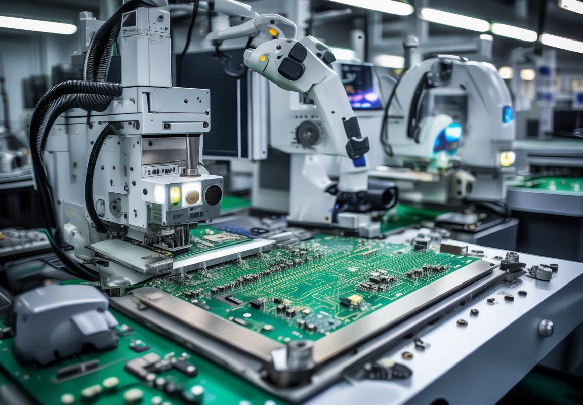
The Automation of Component PlacementOne of the most significant advancements in PCB manufacturing is the automation of component placement. Automated Pick and Place machines, often referred to as P&P machines, have replaced the manual process of placing components on the board. These machines use a robot arm to pick up components from a tape or reel and place them onto the board with incredible precision. The automation not only speeds up the process but also ensures that each component is correctly aligned, reducing the number of errors and reworks.
Printing with PrecisionThe printing stage of PCB manufacturing, where the circuit patterns are transferred onto the board, has also seen a transformation with the advent of automation. Computer-Controlled machines are now used to apply the soldermask, solder paste, and copper patterns with great accuracy. These systems use stepper motors or servo motors to control the placement of the squeegee, ensuring that every line and pad is uniformly coated. This level of precision is difficult to achieve manually, and automation has made it a standard in the industry.
Automated Drilling and RoutingThe drilling process is another area where automation has made a significant impact. Automated drilling machines are designed to drill precise holes in the board, which are then used for component mounting and electrical connections. These machines can drill at high speeds while maintaining consistent hole sizes and placements. The automated routing process follows suit, cutting the copper traces with precision to connect the components. The combination of drilling and routing automation ensures that the boards are ready for the next stage without any manual intervention.
Inspection and Quality ControlQuality is a cornerstone in PCB manufacturing, and automation has enhanced the quality control process. Automated optical inspection (AOI) systems are used to scan the boards for defects such as shorts, opens, and misplacements. These systems can detect issues that are not visible to the human eye, ensuring that only defect-free boards move forward in the production line. Automated X-ray inspection (AXI) takes quality control a step further by detecting hidden defects within the board’s layers, which is crucial for high-density interconnect (HDI) PCBs.
Reflow Soldering and Wave SolderingSoldering is a critical step in PCB assembly, and automation has brought efficiency and consistency to this process. Reflow soldering machines heat the boards to melt the solder paste, which then solidifies, creating the electrical connections. These machines can handle a high volume of boards and ensure that the soldering process is uniform across the entire board. Wave soldering, another common soldering technique, uses a wave of molten solder to make electrical connections. Automated wave soldering systems ensure that the soldering process is consistent and reliable.
Innovations in Assembly and TestingAutomation extends beyond the basic manufacturing stages. In the assembly process, machines can solder and test components simultaneously, reducing the time required for each board. Automated test equipment (ATE) is used to verify the functionality of the PCB after assembly, ensuring that it meets the required specifications. These systems can perform a wide range of tests, from simple continuity checks to complex functional tests, all with high accuracy and speed.
Flexibility and ScalabilityOne of the advantages of automation in PCB production is its flexibility and scalability. Modern automated systems can be easily reconfigured to produce different types of PCBs, from simple to complex. As the demand for PCBs varies, these systems can adjust production volumes accordingly, ensuring that the factory can cater to both small and large orders without compromising quality.
In conclusion, automation has become an integral part of PCB production, improving efficiency, accuracy, and quality. From component placement to soldering and testing, each stage of the PCB manufacturing process benefits from automated technologies. As the electronics industry continues to evolve, the role of automation will likely become even more crucial in meeting the demands of a highly competitive and rapidly changing market.
Quality Control: Ensuring Perfection in Every Board
In the intricate world of printed circuit board (PCB) manufacturing, the quest for perfection is relentless. Each layer of a PCB is meticulously crafted to ensure the board performs its intended function without fail. This pursuit of excellence is where quality control (QC) steps in, acting as the vigilant guardian of every board’s integrity.
Precision is paramount in the QC process, starting with the arrival of raw materials. High-quality copper foil, dielectric materials, and other components must undergo rigorous checks to confirm they meet the strict specifications. Any deviation can compromise the board’s performance, so inspectors scrutinize each batch with a fine-tooth comb.
The boards themselves are subjected to a series of tests as they progress through the manufacturing process. These tests include visual inspections, electrical tests, and mechanical checks. Visual inspections look for imperfections like shorts, opens, or lifted pads, while electrical tests ensure the correct resistance, capacitance, and inductance values are present. Mechanical checks measure the board’s durability, bend resistance, and flexibility.
During the etching stage, the PCB’s copper patterns are defined. Quality control personnel watch for uniformity in the etching process, ensuring that the copper traces are clean and precise. Any inconsistencies could lead to signal integrity issues or mechanical weaknesses.
Once the etching is complete, the board moves to the drilling phase, where holes are punched for components. Quality control is not just about checking the size and shape of the holes; it also involves ensuring the holes are positioned accurately according to the PCB design. Misaligned holes can lead to assembly errors and even damage to the components.
The solder mask application is another critical step. This layer protects the copper traces from environmental damage and prevents unintended soldering. QC checks the solder mask’s adhesion, thickness, and edge definition to guarantee it provides the necessary protection.
The placement of components is a delicate process, and quality control is essential here as well. Automated machines are programmed with high precision, but they can still encounter issues. Inspectors monitor the placement to ensure every component is correctly positioned and oriented. Any errors could affect the board’s functionality or longevity.
After components are placed, they are reflow soldered. Quality control teams watch for consistent solder joints, free of bridges or cold solder points. These joints are the backbone of the PCB, and any flaws can cause intermittent connections or failure.
The final assembly of the PCB is a critical moment for quality control. Every trace, pad, and component is re-examined to ensure everything is in its right place. Inspectors also check for any post-soldering defects, such as discoloration or bubbling, which can indicate issues with the soldering process.
Functional testing is perhaps the most critical phase of quality control. Boards are tested to ensure they meet the electrical specifications and can handle the intended loads. These tests can include performance checks, thermal analysis, and environmental stress screenings. If a board fails any of these tests, it is sent back for repair or, in severe cases, discarded.
Beyond these standard checks, many PCB manufacturers implement additional quality control measures. They might use statistical process control (SPC) to monitor the performance of the manufacturing line over time, ensuring that any trends toward quality issues are identified and addressed promptly.
The quality control process is not just about catching defects; it’s also about continuous improvement. Manufacturers gather data from QC reports to identify areas where the process can be refined or where training is needed. This data-driven approach allows for a continuous evolution in the manufacturing process, leading to higher quality boards and increased customer satisfaction.
In conclusion, the role of quality control in PCB production is multifaceted. It ensures that each board meets the highest standards of performance and reliability, from the raw materials to the final product. By meticulously inspecting every step of the process, manufacturers can provide customers with a product they can trust to perform as intended, time after time.
The Evolution of PCB Design: From Simple to Complex
In the realm of electronics, the evolution of printed circuit board (PCB) design has been a testament to human ingenuity and technological advancements. The journey from simple to complex PCB designs reflects the ever-growing demands of the industry and the relentless pursuit of innovation.
The early days of PCB design were characterized by simplicity. These early boards, often seen in vintage electronics, were straightforward in their layout and functionality. They featured a single layer with copper traces that connected components, which were typically through-hole mounted. The simplicity of these boards made them cost-effective and easy to manufacture, but they were limited in terms of complexity and performance.
As technology progressed, so did the PCB designs. The introduction of multi-layer PCBs marked a significant milestone. These boards allowed for more intricate layouts, enabling engineers to place components on different layers and create complex circuits with better signal integrity. The ability to route traces on multiple layers meant that circuits could be made more compact and efficient, which was crucial for the development of smaller, more powerful devices.
The evolution of PCB design didn’t stop there. The advent of surface mount technology (SMT) brought about a new level of complexity. With SMT, components were mounted directly onto the surface of the PCB, reducing the board’s thickness and allowing for higher component density. This shift from through-hole to SMT also facilitated the creation of finer lines and spaces, enabling even more intricate circuitry.
As PCB designs became more complex, the need for advanced software tools became apparent. CAD (Computer-Aided Design) software emerged as an essential tool for engineers, allowing them to design and simulate PCBs with ease. These programs could handle the intricate details of high-density interconnect (HDI) PCBs, which feature extremely fine lines and spaces, often less than 10 micrometers.
With the rise of smartphones, tablets, and other portable devices, the demand for high-performance PCBs grew exponentially. This led to the development of advanced materials and manufacturing processes. For instance, high-frequency PCBs were designed to handle the higher speeds and frequencies required for modern wireless communication. These PCBs often use materials like Rogers RT/duroid and are manufactured with precision to ensure optimal performance.
The complexity of PCB design has also given rise to specialized PCBs that cater to specific applications. For example, rigid-flex PCBs combine the rigid and flexible properties of materials, making them ideal for use in devices that bend or fold, such as smartphones. Similarly, high-reliability PCBs are designed for harsh environments, such as aerospace and automotive industries, where extreme conditions are the norm.
Moreover, the integration of components on PCBs has reached new heights. Systems-in-Package (SiP) technology allows for the integration of multiple chips into a single package, reducing size and improving performance. This has become particularly important in the development of high-end electronics, where every millimeter counts.
As PCB designs continue to evolve, new challenges and opportunities arise. The demand for faster, more efficient, and more powerful devices drives engineers to push the boundaries of PCB design. This includes the use of innovative materials, such as graphene, which could revolutionize the way PCBs are made and used.
In conclusion, the evolution of PCB design has been a fascinating journey from simple, single-layer boards to complex, multi-layer, high-density circuits. Each step in this evolution has been driven by the needs of the electronics industry and the relentless pursuit of innovation. As technology continues to advance, we can expect to see even more sophisticated PCB designs that will shape the future of electronics.
Sustainability in PCB Factories: A Greener Approach
In the ever-evolving landscape of electronics manufacturing, sustainability has become a cornerstone of progress. PCB factories, once solely focused on efficiency and cost-effectiveness, are now embracing eco-friendly practices to reduce their environmental footprint. Here’s a look at how these facilities are adopting greener approaches:
The shift towards sustainability in PCB factories often begins with the selection of raw materials. Suppliers are now scrutinized for their commitment to environmentally friendly sourcing. Recycled materials and those derived from renewable resources are preferred over traditional, non-renewable options. This change ensures that the initial stages of PCB production are inherently greener.
Efficient use of energy is another key aspect of sustainability. PCB factories have invested in advanced lighting systems that use LED technology, which consumes significantly less power than traditional bulbs. Solar panels and wind turbines are also being installed to harness renewable energy sources, reducing the reliance on fossil fuels.
Waste management is a critical component of sustainability efforts. Instead of disposing of PCB manufacturing waste in landfills, factories are finding innovative ways to recycle and repurpose materials. Chemicals used in the etching process are treated and reused, minimizing the amount of hazardous waste. Even the smallest particles of copper are collected and melted down for future use.
The design phase of PCBs has also undergone a transformation to embrace sustainability. Engineers are now incorporating “green” materials into their designs, such as halogen-free laminates and lead-free solders. These materials are not only better for the environment but also improve the longevity and reliability of the PCBs.
In the realm of process optimization, PCB factories are constantly seeking ways to reduce water usage. Water-efficient systems and recycling processes are employed to minimize waste and ensure that every drop is used effectively. The water that is used in cleaning and rinsing stages is treated and reused, significantly cutting down on freshwater consumption.
Employee training is another area where sustainability is being prioritized. Workers are educated on the importance of eco-friendly practices and how their daily actions can contribute to a greener factory. This includes proper handling and disposal of hazardous materials, as well as energy-saving measures in the workplace.
The packaging of PCBs is also being reevaluated. Companies are moving away from single-use plastics and opting for recyclable or biodegradable materials. This not only reduces waste but also ensures that the PCBs themselves are not contributing to pollution during transportation and storage.
Technology plays a pivotal role in sustainability initiatives. PCB factories are integrating advanced software to optimize production processes, reducing waste and improving efficiency. This includes predictive maintenance systems that can anticipate and prevent equipment failures, thereby reducing downtime and the need for emergency repairs.
As the electronics industry continues to grow, the pressure to innovate and remain competitive is immense. However, PCB factories are proving that sustainability can be a driving force behind innovation. By investing in research and development, these factories are developing new, more sustainable manufacturing techniques and materials.
The end-of-life phase of PCBs is also being addressed. With the help of industry-wide recycling programs, PCBs can be disassembled and the valuable materials recovered. This not only closes the loop on the product lifecycle but also reduces the need for mining new materials.
In conclusion, the journey towards sustainability in PCB factories is a multifaceted one, encompassing every aspect of the manufacturing process. From the sourcing of raw materials to the final disposal of products, each step is being carefully considered to minimize environmental impact. As the industry continues to evolve, it’s clear that a greener approach is not just a trend; it’s a necessity for the future of electronics manufacturing.
The Impact of PCBs on Various Industries
In the digital age, printed circuit boards (PCBs) have become the backbone of countless industries, revolutionizing the way products are designed, manufactured, and operated. Their impact is profound, touching almost every sector in one way or another.
The electronics industry, of course, is the most direct recipient of PCBs’ influence. These boards are the heart of every electronic device, from the smallest microchip to the largest server farm. They facilitate the miniaturization of components, allowing for sleeker, more efficient devices. The evolution of PCBs has enabled the development of advanced technologies such as smartphones, laptops, and IoT devices, which have become integral to our daily lives.
In the automotive sector, PCBs have transformed vehicle design and performance. Modern cars are equipped with a myriad of electronic systems that rely on PCBs for their operation. These include navigation systems, engine management units, and advanced driver-assistance systems (ADAS). PCBs have made it possible to integrate complex functionalities into vehicles, enhancing safety, efficiency, and convenience.
The medical industry has also been significantly impacted by PCBs. In medical devices, PCBs are crucial for ensuring reliable and precise performance. They are used in everything from heart monitors and MRI machines to insulin pumps and pacemakers. The precision and durability of PCBs are essential in these applications, as they directly affect patient care and well-being.
In the aerospace industry, PCBs are integral to the development of sophisticated aircraft systems. They are used in navigation, communication, and control systems, where reliability is paramount. The lightweight and high-performance nature of PCBs has allowed for the creation of more efficient and advanced aircraft, contributing to the industry’s growth and innovation.
The telecommunications industry has seen a surge in demand for PCBs with the advent of 5G technology. These boards are essential for the deployment of 5G networks, which require higher speeds and greater bandwidth. PCBs enable the miniaturization of antennas and other components, making it possible to deploy the infrastructure needed for 5G connectivity.
In the consumer electronics market, PCBs have driven innovation in products like gaming consoles, smart home devices, and wearable technology. These devices are becoming more sophisticated, and PCBs are the foundation for integrating multiple functions into a single unit. The demand for PCBs in this sector is only expected to grow as consumers seek more integrated and intelligent devices.
The defense industry also relies heavily on PCBs for the development of military equipment. From communication systems to radar technology, PCBs are used to create complex and reliable systems that are critical for national security. The precision and security of PCBs are paramount in this context, as they are often used in environments where failure is not an option.
The environmental impact of PCBs is another area where their influence is felt. As awareness of sustainability grows, PCB manufacturers are increasingly focusing on eco-friendly practices. This includes the use of recyclable materials, energy-efficient manufacturing processes, and responsible disposal methods. The industry is also researching alternative materials that are less harmful to the environment.
In the field of research and development, PCBs play a crucial role in prototyping and testing new technologies. Scientists and engineers use PCBs to create temporary circuits that can be easily modified and tested. This flexibility is essential for the iterative process of innovation, allowing for rapid development and refinement of new ideas.
The impact of PCBs on various industries is undeniable. They have become a cornerstone of modern technology, enabling the creation of complex, efficient, and reliable systems. As industries continue to evolve, the role of PCBs will likely become even more integral, driving further innovation and advancement.
Challenges and Innovations in PCB Manufacturing
In the intricate world of PCB manufacturing, challenges and innovations go hand in hand. As technology advances, so does the complexity of the processes involved. Navigating these complexities requires a blend of creative problem-solving and cutting-edge technologies.
The demand for smaller, more efficient PCBs has pushed manufacturers to develop innovative techniques. Miniaturization is not just about shrinking the size of the boards but also about enhancing their performance. To achieve this, manufacturers are exploring new materials and manufacturing processes that can handle the increased density of components.
One significant challenge is the need for high precision in PCB manufacturing. With components becoming ever smaller, the tolerances for errors are shrinking. Advanced machinery and software are being employed to ensure that every aspect of the PCB, from the copper traces to the solder joints, meets the exacting standards required.
Innovation in PCB manufacturing often involves the development of new materials. For instance, the use of high-frequency materials has become crucial for applications in the telecommunications and aerospace industries. These materials help to reduce signal loss and improve the overall performance of the PCB.
Another challenge is the environmental impact of PCB manufacturing. The chemicals used in the etching and cleaning processes can be harmful to both the environment and the health of workers. To address this, manufacturers are investing in green technologies that reduce waste and minimize the use of harmful substances.
The complexity of PCB design has also introduced new challenges. As boards become more intricate, the need for sophisticated software to design and simulate their performance becomes paramount. Software advancements have enabled designers to visualize and predict how PCBs will perform under various conditions, leading to more reliable and efficient products.
One innovation that has revolutionized PCB manufacturing is the introduction of 3D printing. While not yet widely adopted for mass production, 3D printing offers the potential to create highly customized PCBs with complex geometries. This technology could potentially reduce the time and cost associated with traditional PCB manufacturing.
Moreover, the integration of sensors and smart technologies into PCBs has opened up new possibilities. These smart PCBs can monitor their own health and performance, providing valuable data for maintenance and upgrades. This integration requires a new level of precision and reliability in PCB manufacturing.
The challenge of maintaining high standards while scaling up production is another area where innovation is key. As demand for PCBs continues to grow, manufacturers must find ways to increase output without compromising quality. This often involves optimizing production lines, automating processes, and investing in training for the workforce.
The challenges in PCB manufacturing are not just technical; they also extend to the supply chain. Ensuring a steady supply of high-quality raw materials is critical, as is maintaining the integrity of the supply chain to prevent disruptions. Innovations in supply chain management are helping manufacturers to stay ahead of these challenges.
In conclusion, the PCB manufacturing industry is a testament to human ingenuity and resilience. Despite the myriad challenges, from the smallest details of board design to the environmental impact of production, manufacturers continue to innovate and push the boundaries of what is possible. The result is a testament to the power of technology and the dedication of those who work tirelessly to bring these innovations to life.
The Future of the Integrated Circuit Board Factory
In the ever-evolving landscape of technology, the integrated circuit board (ICB) factory stands as a testament to human ingenuity and the relentless pursuit of innovation. These factories are the beating heart of the electronics industry, where complex circuits are meticulously crafted onto thin, durable boards that power everything from smartphones to medical devices. The future of these factories is poised to be transformative, driven by advancements in automation, sustainability, and the relentless demand for faster, smaller, and more efficient PCBs.
The relentless push for miniaturization has led to the development of advanced manufacturing techniques that allow for the creation of PCBs with features that were once unimaginable. These advancements are not just limited to the physical size of the boards but also to their functionality and reliability. As the demand for high-speed, high-frequency, and multi-layer PCBs grows, so does the complexity of the manufacturing process.
One of the most significant changes in PCB manufacturing is the integration of robotics and AI. These technologies are not just streamlining production but also enabling the creation of PCBs with unprecedented precision. Robots can handle tasks that were once the purview of skilled technicians, such as placing and soldering tiny components, which reduces errors and increases throughput. AI algorithms can predict potential defects before they occur, ensuring that each board meets the stringent quality standards set by the industry.
Sustainability has become a cornerstone in the PCB manufacturing industry. As environmental concerns grow, factories are adopting greener practices to reduce their carbon footprint. This includes the use of eco-friendly materials, water recycling systems, and energy-efficient manufacturing processes. The shift towards sustainability is not just a moral imperative but also a business advantage, as consumers and regulators increasingly demand responsible manufacturing practices.
The impact of PCBs on various industries is profound. In the automotive sector, PCBs are crucial for the development of autonomous vehicles, where they enable the complex systems that control everything from the engine to the braking system. In the medical field, PCBs are integral to the creation of life-saving devices, such as defibrillators and MRI machines. The entertainment industry relies on PCBs to deliver high-definition visuals and immersive sound experiences, while the aerospace industry depends on them for the intricate circuits that power modern aircraft.
However, with this profound impact comes a set of challenges. One of the most pressing issues is the demand for faster production cycles without compromising quality. This challenge is met with continuous innovations in manufacturing processes, such as the development of new materials that can withstand higher temperatures and voltages, and the use of advanced etching techniques that allow for more intricate designs.
The complexity of PCB designs has also introduced new challenges. As circuits become more dense and interconnected, the risk of errors and failures increases. To combat this, manufacturers are investing in advanced testing equipment and software that can analyze the performance of PCBs under various conditions. These tools not only detect defects but also provide insights into the design process, allowing engineers to make improvements before the boards even leave the factory.
Innovation in PCB manufacturing is not confined to the production floor. The industry is also seeing a surge in research and development efforts aimed at creating new materials and processes. Graphene, for example, is being explored for its potential to create PCBs with superior thermal conductivity and mechanical strength. Additionally, nanotechnology is being used to develop new types of conductive inks and adhesives that can handle more complex and delicate circuits.
The future of the integrated circuit board factory is one of continuous transformation. As technology advances, so too will the capabilities of these factories. We can expect to see even greater integration of robotics and AI, as well as the development of new manufacturing techniques that push the boundaries of what is possible. The industry will also need to adapt to changing market demands, regulatory requirements, and environmental concerns.
In conclusion, the future of the integrated circuit board factory is bright, filled with opportunities for innovation and growth. As the demand for advanced electronics continues to rise, these factories will play a pivotal role in shaping the technological landscape of the future. The key will be the ability to balance technological advancements with sustainable practices, ensuring that the industry remains at the forefront of progress while also being mindful of its impact on the world around us.