As the digital age advances, the role of integrated circuit board (ICB) factories in shaping our technological landscape becomes increasingly evident. These factories, often unseen by the public eye, are the silent architects of the devices that power our lives. Today, let’s delve into the intricate world of ICB manufacturing, exploring the evolution, challenges, and innovations that drive this critical industry forward.
The Evolution of the Integrated Circuit Board Factory
In the world of technology, few advancements have had as profound an impact as the integrated circuit (IC) board. Over the years, the PCB factory has transformed from a modest workshop into a cornerstone of modern electronics. Let’s delve into the fascinating journey of how the IC board factory has evolved.
Once upon a time, circuit boards were hand-soldered with individual components, a labor-intensive and time-consuming process. The advent of printed circuit boards (PCBs) revolutionized this field. These boards, with their precise layouts and pre-drilled holes, allowed for faster and more efficient assembly.
As the demand for electronic devices surged, so did the need for more sophisticated PCBs. The 1970s saw the introduction of multi-layer PCBs, which enabled complex circuits to be packed onto a single board. This development not only reduced the size of electronic devices but also enhanced their functionality.
The 1980s brought about a new era with the introduction of surface mount technology (SMT). SMT allowed for smaller components to be placed directly onto the PCB, further shrinking the size of electronic devices. This shift in manufacturing processes led to increased efficiency and reduced production costs.
With the dawn of the 1990s, PCB factories began to embrace automation. Robotics and computer-aided design (CAD) systems took over many tasks, such as component placement and soldering. This not only improved the quality of the final product but also increased production speeds.
As the 21st century rolled in, the industry saw another leap forward with the introduction of high-speed PCB manufacturing. Today’s PCB factories can produce complex boards with precision and speed, often in a fraction of the time it took just a few decades ago.
One of the most significant advancements in PCB manufacturing has been the use of advanced materials. High-frequency materials, for instance, enable PCBs to function at higher frequencies without signal loss. This has been crucial for the development of modern communication technologies like Wi-Fi and Bluetooth.
Environmental concerns have also played a pivotal role in shaping the evolution of PCB factories. As awareness of sustainability grew, manufacturers started adopting eco-friendly practices. This includes using lead-free solders, reducing waste, and implementing energy-efficient processes.
Another key factor in the evolution of PCB factories has been the rise of customization. With the advent of online platforms, customers can now design their own PCBs with ease. This has opened up new opportunities for innovation and has allowed PCB factories to cater to a wider range of applications.
The rise of the Internet of Things (IoT) has further fueled the growth of the PCB industry. As more devices become interconnected, the demand for high-quality, reliable PCBs has surged. PCB factories are now producing boards that are not only compact but also capable of handling vast amounts of data.
Innovation in PCB design and manufacturing continues to push the boundaries of what is possible. Miniaturization, high-speed data transmission, and advanced packaging technologies are just a few areas where the industry is making significant strides.
The evolution of the IC board factory is a testament to human ingenuity and the relentless pursuit of progress. From the early days of hand-soldered circuits to the cutting-edge PCBs of today, the industry has come a long way. As we look to the future, it’s clear that the PCB factory will continue to play a vital role in shaping the world of electronics.
Understanding the Heart of Modern Electronics
The integrated circuit board, often simply referred to as the PCB, is the backbone of modern electronics. It’s a marvel of engineering that has transformed the way we interact with the world around us. Let’s delve into the intricacies and significance of this crucial component.
In the early days of electronics, circuits were built using a patchwork of wires and resistors, a labor-intensive and error-prone process. But as technology advanced, so did the need for a more efficient and reliable method of connecting components. This led to the birth of the PCB, a flat board with conductive pathways etched onto its surface.
These pathways, known as traces, are meticulously designed to carry electrical signals between various components. The PCB serves as a roadmap for the flow of electricity, ensuring that each part of the circuit operates as intended. Over time, PCBs have become increasingly sophisticated, with the ability to house complex circuits on a single board.
The materials used in PCB manufacturing have also evolved. Early boards were made from materials like paper and fabric, but today, they are predominantly made from a non-conductive base material called FR-4. This composite material provides both rigidity and durability, making it ideal for the demands of modern electronics.
As technology progressed, the need for smaller, more efficient PCBs became apparent. This led to the development of finer lines and spaces, allowing for higher density and more complex circuits. Today, PCBs can be as small as a few square millimeters, packing thousands of components into a compact space.
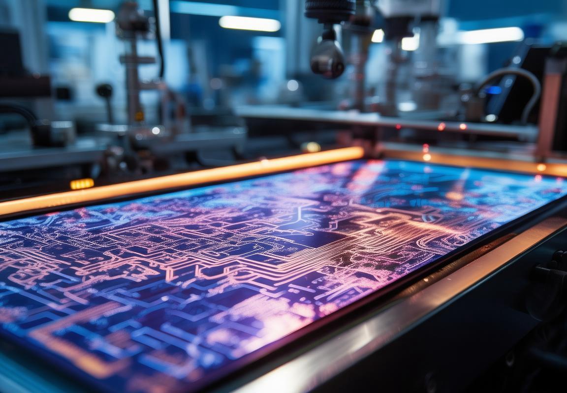
The design process of a PCB is a meticulous one. Engineers use specialized software to lay out the circuit, determining the placement of components and the routing of the traces. This design is then transferred onto the PCB substrate, usually through a process called photolithography. This process involves exposing a layer of photosensitive material to light, which hardens in areas where it’s exposed, allowing for the etching of the traces.
Once the design is transferred, the PCB enters the etching phase. Chemicals are used to remove the unexposed material, leaving behind the copper traces. This process must be precise to avoid any shorts or open circuits, which could render the PCB ineffective.
Another critical aspect of PCB manufacturing is the drilling of holes. These holes, known as vias, allow electrical connections between different layers of the PCB. The drilling process must be precise to ensure that the vias are correctly aligned with the traces on each layer.
After the drilling and etching, the PCB undergoes a series of surface finishing processes. These can include the application of soldermask, which protects the copper from oxidation and soldering defects, and silk screening, which provides identification for components and other information.
The next step is the assembly of the PCB. Components are placed onto the board using automated machines, which then solder them in place. This assembly process must be incredibly accurate, as even a small misalignment can lead to a malfunctioning device.
Once assembled, the PCB is subjected to rigorous testing to ensure its functionality. This testing can include everything from basic connectivity checks to more complex simulations that mimic real-world conditions. Only after passing these tests is the PCB deemed ready for use.
The impact of PCBs on modern electronics is immense. They have enabled the miniaturization of devices, improved their performance, and reduced their cost. Without PCBs, our smartphones, computers, and countless other gadgets would be impractical or impossible.
The evolution of the PCB has been a testament to human ingenuity and the relentless pursuit of innovation. As we continue to push the boundaries of technology, the PCB will undoubtedly continue to play a pivotal role in shaping the future of electronics. Its ability to seamlessly integrate complex circuits into a single, flat board is a testament to the incredible advancements we’ve made in the field of electronics.
Key Processes in an Integrated Circuit Board Factory
In the intricate dance of modern electronics, the integrated circuit board (ICB) factory plays a pivotal role. These factories are the beating heart of the tech industry, where precision and innovation converge to produce the intricate components that power our devices. Let’s delve into the key processes that occur within these manufacturing sanctuaries.
The journey of an integrated circuit board begins with the design phase, where engineers meticulously craft the blueprint for the board’s layout. This is where the “silk screen” process comes into play, where a thin layer of ink is applied to the board to create a visual representation of the component placements.
Once the silk screening is complete, the boards move on to the etching process. This involves using chemical solutions to remove unwanted copper from the board, leaving behind the intricate patterns that will serve as the pathways for electrical signals. The etching process is a delicate balance of chemical reaction and controlled exposure, ensuring the precision required for complex circuits.
After etching, the boards are cleaned and primed for the next step: the lamination process. Lamination involves bonding layers of substrate material together, often with a thin layer of copper sandwiched in between. This process is crucial for the board’s durability and electrical integrity, as it creates a solid foundation for the components to be mounted on.
Once the substrate is lamination complete, the boards are ready for the drilling phase. High-speed drills pierce through the copper layers, creating the necessary holes for components like resistors, capacitors, and integrated circuits to be inserted. This step requires extreme precision, as the placement of these holes is critical for the board’s functionality.
The drilled boards then move to the electroplating stage. Here, a layer of copper is plated onto the exposed copper pads and the holes, creating a conductive path for the electrical signals. This process is repeated to achieve the desired thickness, ensuring reliable connections between components.
After electroplating, the boards are treated with a chemical etching process to remove any excess copper. This step is crucial for ensuring that the board’s surface is clean and free of any impurities that could disrupt the circuit’s performance.
The next step involves the application of a solder mask. This layer of material is applied to the board to protect the copper from oxidation and to provide a non-conductive surface for the placement of components. The solder mask is typically green, but it can come in various colors to match specific design requirements.
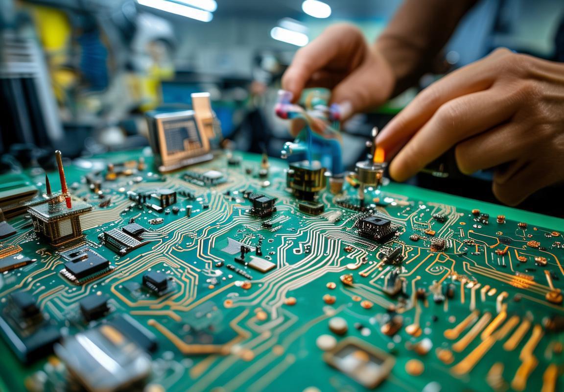
Once the solder mask is cured, the board is ready for component placement. This is where the pick-and-place machines come into play, accurately placing each component onto the board in the correct orientation. The precision of these machines is crucial, as even a small misalignment can render the board non-functional.
After placement, the components are soldered onto the board using reflow soldering. This process involves heating the board to melt the solder paste, which then solidifies to create a permanent bond between the component and the board. The temperature must be carefully controlled to ensure a good solder joint without damaging the components.
The final steps involve the testing and quality control processes. Boards are subjected to various tests to ensure they meet the required specifications, including electrical performance and durability. Any defects are flagged, and the boards are either repaired or discarded.
Throughout this intricate process, the ICB factory relies on a combination of cutting-edge technology and skilled labor. Automation has revolutionized many aspects of PCB manufacturing, but the human touch is still invaluable in quality control and problem-solving.
In summary, the key processes in an ICB factory are a testament to the meticulous attention to detail and technological prowess required to produce the complex integrated circuit boards that are the backbone of modern electronics. From design to assembly and testing, each step is crucial for the reliability and functionality of the end product.
The Role of Technology in PCB Manufacturing
In the realm of electronic manufacturing, the role of technology is paramount, especially within the production of printed circuit boards (PCBs). These intricate boards are the backbone of modern electronics, providing the pathways for electrical signals to flow efficiently. Here’s a glimpse into how technology shapes PCB manufacturing:
The precision required in PCB production is unmatched, and it all begins with the design phase. Advanced CAD (Computer-Aided Design) software allows engineers to create detailed layouts with incredible accuracy. These designs are the blueprints for the physical boards, and they must account for the smallest of details to ensure optimal performance.
Laser cutting technology has revolutionized the way PCBs are manufactured. It offers unparalleled precision, allowing for intricate routing and etching processes that were once impossible with traditional methods. The ability to cut complex patterns with a laser ensures that every trace and via is perfectly aligned, contributing to the board’s reliability.
Chemical etching, another critical process, relies heavily on technological advancements. Today’s etching systems use highly controlled environments and advanced chemical solutions to accurately remove copper from the board’s base material. The precision of this process is vital, as it determines the quality of the copper traces that will conduct the electrical current.
The advent of robotic assembly has drastically increased efficiency and reduced errors in PCB manufacturing. Robots can place components with extreme precision, far surpassing the capabilities of human hands. This automation not only speeds up production but also ensures that each component is placed correctly, reducing the risk of faulty connections.
Inkjet printing technology has made it possible to print fine lines and precise patterns on PCBs with ease. This is particularly important for high-density interconnect (HDI) PCBs, which require smaller vias and finer lines. Inkjet printing provides a level of detail that was once reserved for specialized, and more expensive, processes.
Technology has also brought about significant advancements in the testing phase of PCB manufacturing. Automated testing equipment can scan boards for defects, such as shorts, opens, and copper burrs, ensuring that only the highest quality PCBs leave the factory. This level of quality control is essential for the longevity and reliability of electronic devices.
Another technological marvel is the use of 3D printing in PCB manufacturing. While still in the developmental stages, 3D printing has the potential to revolutionize the way PCBs are made. It allows for the creation of complex geometries and structures that are not feasible with traditional manufacturing techniques. This could lead to more efficient and compact electronic devices.
The material science behind PCBs has also seen significant advancements. New materials, such as high-frequency laminates, are being developed to accommodate the increasing demand for faster and more reliable electronic devices. These materials not only enhance the performance of PCBs but also extend their lifespan in harsh environments.
The environmental aspect of PCB manufacturing has also been transformed by technology. More energy-efficient systems and sustainable materials are being used to reduce the carbon footprint of PCB production. This not only benefits the environment but also appeals to environmentally conscious customers.
In the realm of PCB manufacturing, technology is not just a tool but a driving force behind innovation. From the design phase to the final assembly, every aspect of PCB production is influenced by technological advancements. These innovations not only improve the quality and efficiency of PCBs but also pave the way for the next generation of electronic devices. As technology continues to evolve, so too will the capabilities and reliability of PCBs, ensuring that they remain the heart of modern electronics.
Challenges and Innovations in PCB Production
In the world of PCB (Printed Circuit Board) production, challenges and innovations go hand in hand. As technology advances, the demands for smaller, more efficient, and higher-quality PCBs continue to rise. Let’s delve into the various hurdles faced and the groundbreaking solutions that have emerged.
The Shrinking PCBs
The push for miniaturization has been relentless. PCBs that were once the size of a deck of cards are now as small as a thumbnail. This miniaturization has led to increased complexity in the design and manufacturing process. Engineers must navigate the delicate balance of signal integrity, heat dissipation, and component placement. Innovations such as high-density interconnect (HDI) technology have allowed for finer lines and spaces, enabling the creation of smaller PCBs without compromising performance.
Environmental Concerns
As PCB production scales up, environmental concerns have become more pronounced. Traditional manufacturing processes can be harmful to both the environment and human health. The industry has responded by developing greener alternatives. For instance, lead-free solders are now the norm, reducing the environmental impact. Additionally, recycling programs have been implemented to recover and reuse precious materials from discarded PCBs.
Heat Management
Heat is the enemy of electronic devices, and PCBs are no exception. As devices become more powerful, they generate more heat, which can lead to reduced lifespan and reliability. PCB manufacturers have introduced several innovative solutions to manage heat. Heat sinks, thermal vias, and improved material choices, such as using copper with higher thermal conductivity, have all been employed to keep the components cool and functioning optimally.
Complex Design Requirements
Designers are constantly pushing the boundaries of what PCBs can do. They are expected to integrate more components, achieve higher frequencies, and accommodate new technologies like flexible circuits and multi-layer boards. To meet these demands, PCB manufacturers have developed advanced design software that allows for complex simulations and real-time design verification. These tools help ensure that the PCBs can handle the rigorous demands of modern electronics.
Automated Assembly
Automation has become a cornerstone of PCB production. Manual assembly is slow and prone to error, so factories have invested heavily in automated systems. Pick-and-place machines can place thousands of components per hour with precision. Soldering robots ensure consistent and reliable joints. These automated processes not only increase efficiency but also reduce labor costs and improve the overall quality of the PCBs.
Material Advancements
The materials used in PCB production are continually evolving. New materials are being developed to offer better thermal conductivity, electrical insulation, and flexibility. For example, polyimide is a material that can withstand extreme temperatures and is used in high-performance PCBs. Innovations in material science are making PCBs more durable and capable of withstanding harsh conditions.
Quality Control
The quality of a PCB is crucial for the reliability of the electronic device it powers. Manufacturers have implemented rigorous quality control processes to ensure that each PCB meets the highest standards. Advanced inspection technologies, such as X-ray machines and automated optical inspection (AOI) systems, are used to detect defects at an early stage. These tools help reduce the number of faulty PCBs and improve overall yield.
Supply Chain Management
The PCB manufacturing process is highly dependent on a complex supply chain. Ensuring that all components are available, reliable, and of high quality is a significant challenge. Innovations in supply chain management, such as real-time tracking and predictive analytics, have helped manufacturers anticipate demand and maintain inventory levels. This approach minimizes downtime and ensures a smooth production flow.
Regulatory Compliance
The PCB industry is subject to numerous regulations, both locally and internationally. Ensuring compliance with these laws can be daunting. However, manufacturers are innovating by adopting systems that can track and report on regulatory requirements. This proactive approach helps them stay ahead of potential legal issues and maintain a good reputation in the market.
In conclusion, the challenges in PCB production are vast, but so are the innovations that are being developed to overcome them. From material advancements to automated assembly and environmental concerns, the industry is constantly evolving to meet the demands of modern electronics.
The Impact of Quality Control on PCB Factories
The intricacies of quality control in PCB (Printed Circuit Board) factories are paramount, as these boards are the backbone of countless electronic devices. Here’s a glimpse into how quality control shapes the landscape of PCB production:
Precision in Design VerificationThe process begins with the design of the PCB, where engineers meticulously map out the circuitry. Quality control systems ensure that the designs are accurate, meeting the stringent requirements of various industries. This includes checking for compliance with international standards, such as IPC (Institute of Printed Circuits), and verifying that the design can be manufactured without issues.
Automated Inspection and TestingAs the boards are manufactured, automated inspection tools play a crucial role. Advanced machines can scan the boards for defects such as shorts, opens, and misaligned components. Innovations in machine vision technology have allowed for high-speed, accurate checks, reducing the margin for human error.
Consistency in Material SelectionThe quality of PCBs is heavily dependent on the materials used. Quality control teams rigorously inspect raw materials for purity and compliance with specifications. This includes checking for the right thickness and conductivity of copper foil, the strength of the dielectric substrate, and the precision of component placement.
Environmental ControlThe manufacturing environment itself must be controlled to maintain quality. PCB factories employ cleanrooms to reduce dust and contamination, which can interfere with the circuit’s integrity. Innovations in air filtration systems and humidity control ensure a stable environment for consistent production.
Continuous Process MonitoringThroughout the manufacturing process, continuous monitoring systems keep a watchful eye on the equipment and materials. Sensors can detect variations in temperature, pressure, and chemical levels, allowing for immediate adjustments to maintain quality.
Error Correction and Feedback LoopsWhen defects are found, it’s not just about fixing the immediate problem. Quality control teams analyze the root causes of errors and implement corrective actions. This often involves revising processes, training staff, or updating equipment to prevent future occurrences.
Supplier QualificationThe quality of a PCB is not solely dependent on the factory’s processes. Supplier qualification is a key aspect of quality control. Factories must ensure that their suppliers meet the same high standards, often through audits and regular assessments.
Document Control and TraceabilityEvery aspect of the PCB production process is documented, from the initial design to the final product. This documentation is crucial for traceability, allowing for quick identification of the source of any defects. Innovations in document management systems have made it easier to store, retrieve, and analyze this data.
Client Feedback and ComplianceClient feedback is invaluable for PCB factories. Quality control systems often include mechanisms for collecting and analyzing customer input. This not only helps in improving current products but also in ensuring compliance with industry regulations and client-specific requirements.
Training and Continuous ImprovementInvesting in training is a cornerstone of quality control. Employees are trained on the latest manufacturing techniques, quality standards, and safety procedures. This continuous learning culture fosters innovation and a commitment to excellence.
Innovation in Quality Assurance ToolsThe evolution of technology has brought about new tools for quality assurance. From 3D imaging for inspecting complex boards to AI-driven predictive maintenance, these innovations are transforming how PCB factories manage quality.
Risk Management and Compliance AuditsQuality control is also about managing risks. Regular compliance audits ensure that PCB factories adhere to the necessary regulations and standards. Innovations in risk management software help in identifying potential hazards and planning mitigation strategies.
Quality Control as a Competitive AdvantageUltimately, the rigorous application of quality control in PCB factories is not just about meeting standards; it’s about gaining a competitive edge. High-quality PCBs are less likely to fail in the field, reducing warranty costs and enhancing brand reputation.
The Impact of Quality on Product LifespanThe reliability of PCBs directly influences the lifespan of electronic products. A PCB that undergoes meticulous quality control is more likely to perform consistently over time, contributing to the overall durability and satisfaction of the end-users.
In conclusion, the impact of quality control on PCB factories is profound. It touches every aspect of the production process, from design and materials to the final product and customer satisfaction. The pursuit of excellence in quality control is an ongoing journey that requires innovation, continuous improvement, and a deep understanding of the needs of both clients and the industry.
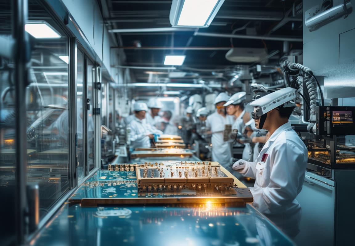
Case Study: A Day in the Life of a PCB Factory
The factory’s hum begins at the crack of dawn, a symphony of whirring machines and bustling workers. The day at the PCB (Printed Circuit Board) factory starts with a sense of purpose, as teams prepare to tackle the intricate art of electronics assembly. Workers don their protective gear, ensuring safety is paramount as they navigate through the factory’s corridors.
The first stop is the incoming inspection area, where a team meticulously examines each batch of raw materials. From high-quality copper foil to precision-crafted circuit patterns, every component is inspected for defects. A single speck of dust or a misaligned trace can spell disaster, so each piece must meet stringent quality standards.
Once the materials pass inspection, they are transported to the etching line. Here, the copper foil is submerged in chemical baths, where a chemical reaction removes the excess material, leaving a precise pattern of copper on the board. The process is precise and delicate, requiring constant monitoring to avoid over-etching or under-etching.
After etching, the boards move to the drilling phase. High-speed drills pierce through the board, creating the necessary holes for components to be mounted. This process is automated, with computer-controlled machines ensuring accuracy and consistency. Workers stand by, ready to intervene if any issues arise, ensuring that the holes are perfectly aligned and the board’s integrity is maintained.
Next, the boards head to the chemical stripping station. Any remaining unwanted copper is removed, leaving a clean surface for the solder mask to be applied. The solder mask, a protective layer, is crucial in preventing shorts and ensuring a smooth flow of electricity. Workers use automated applicators to apply the mask, ensuring even coverage without smudges or gaps.
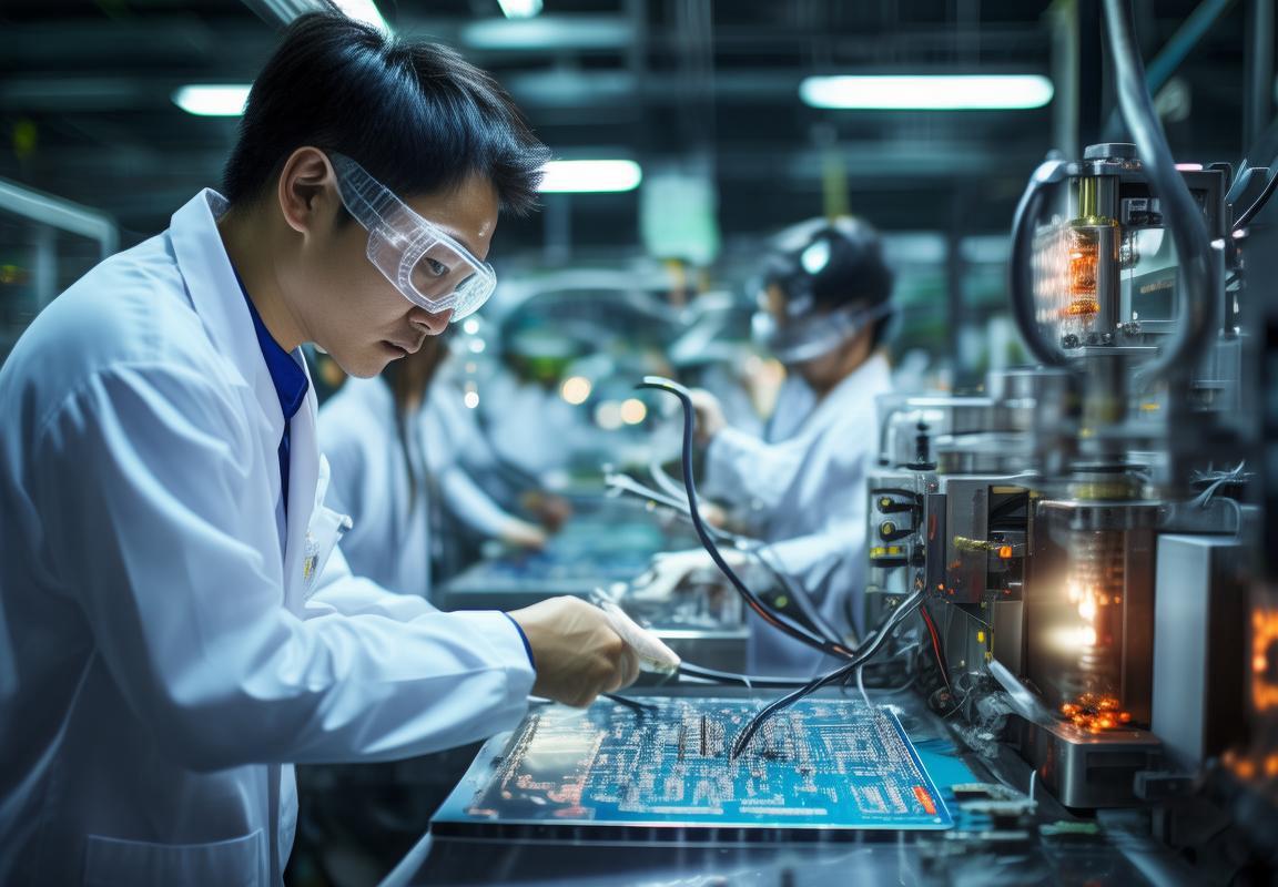
The boards then proceed to the soldering area. Here, skilled technicians use automated pick-and-place machines to place surface-mount devices (SMDs) onto the boards. The precision required is extraordinary, as even the smallest misalignment can affect the board’s performance. Once the components are in place, the boards are subjected to reflow ovens, where a controlled heat cycle melts the solder, securing the components in place.
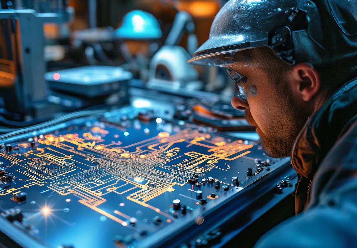
Quality control is a constant presence throughout the day. Teams of inspectors use microscopes to examine the boards under intense light, searching for any imperfections. They check for proper solder joints, clean traces, and ensure that all components are correctly positioned. Any deviation from the standards is flagged, and the boards are sent back for rework or discarded if they fail to meet specifications.
As the day progresses, the boards move through the assembly line, where they are subjected to various tests. Functional tests verify that the circuit operates as intended, while electrical tests measure parameters such as resistance and capacitance. Any board that fails these tests is flagged for further investigation.
The day comes to a close with a final inspection. Workers inspect the finished PCBs, ensuring they meet the customer’s specifications and quality requirements. They package the boards, labeling them with the necessary information and preparing them for shipment.
In the PCB factory, innovation is key. New technologies are constantly being developed to improve the efficiency and quality of production. For instance, advanced laser drilling techniques can create holes with superior precision, reducing the need for manual intervention. Automated inspection systems are becoming more sophisticated, capable of detecting even the most minute defects that were once impossible to spot.
The factory also invests in research and development, exploring new materials and processes that can enhance the performance and longevity of PCBs. One such innovation is the use of high-frequency materials that allow PCBs to operate more efficiently in today’s fast-paced electronics world.
Despite the advancements, challenges remain. The complexity of modern PCBs continues to grow, with increasing demands for smaller, more powerful, and more efficient boards. This necessitates constant training for workers and the adoption of new equipment that can handle the intricate designs. Additionally, environmental concerns have led to the development of eco-friendly materials and processes, which must be balanced with cost and performance.
In the heart of the PCB factory, each day is a testament to human ingenuity and the relentless pursuit of perfection. The workers, machines, and materials all play their part in crafting the backbone of modern electronics, from smartphones to spacecraft. It’s a world where every detail counts, and the impact of quality control is felt at every stage of the production process.
The Future of Integrated Circuit Board Factories
In the ever-evolving landscape of technology, the future of integrated circuit board (ICB) factories is poised to be transformative. As we delve into the potential advancements and shifts in the industry, several key themes emerge, painting a picture of a dynamic and innovative sector.
The integration of advanced robotics and automation is set to revolutionize the production line. Robots, with their precision and speed, are likely to take over repetitive tasks, freeing human technicians to focus on more complex and intricate work. This shift will not only increase efficiency but also reduce the margin for human error, which is crucial in the delicate world of PCB manufacturing.
The rise of smart manufacturing is another significant trend. By incorporating the Internet of Things (IoT) and artificial intelligence (AI), PCB factories can anticipate maintenance needs, optimize production schedules, and even predict potential issues before they arise. This proactive approach to manufacturing ensures a seamless workflow and reduces downtime.
Environmental sustainability is becoming a focal point for many PCB factories. As concerns over carbon footprints and ecological impact grow, manufacturers are investing in green technologies. This includes the use of recycled materials, energy-efficient processes, and water-saving techniques. The future of PCB factories will likely see a more eco-friendly approach to production, balancing technological advancements with environmental responsibility.
The demand for miniaturization and high-density interconnect (HDI) PCBs is driving innovation in the industry. As devices become more compact, PCBs must also shrink in size while maintaining functionality. This push for smaller, more efficient PCBs is prompting the development of new materials and manufacturing techniques that can handle the increased complexity.
The customization of PCBs is also expected to become more prevalent. With the ability to produce PCBs tailored to specific applications, factories will need to be flexible and adaptable. This could involve rapid prototyping capabilities and the ability to quickly adjust designs based on customer feedback, ensuring that each PCB meets the exacting standards of its intended use.
The global supply chain is another area where PCB factories are looking to innovate. As geopolitical tensions and trade disputes continue to impact the flow of goods, factories are exploring ways to localize their supply chains. This could mean sourcing materials closer to home or developing regional manufacturing hubs. The goal is to create a more resilient and less vulnerable supply chain.
Collaboration between PCB manufacturers and other sectors, such as automotive, aerospace, and medical, is on the rise. These industries often have unique requirements for PCBs, and by working closely with them, manufacturers can develop new products and solutions that address these specific needs. This partnership is likely to accelerate as industries become more interconnected.
Data security and privacy are critical concerns in PCB manufacturing. As PCBs are integral to the operation of many devices that handle sensitive information, factories must ensure that their products meet stringent security standards. This includes not only the physical security of the PCB but also the protection of the data that is processed and stored on them.
The future of PCB factories is also about upskilling the workforce. As technology advances, the skills required to operate and maintain PCB manufacturing equipment will evolve. Factories will need to invest in training programs to keep their employees’ skills current and relevant. This could involve on-the-job training, online courses, or even partnerships with educational institutions.
Lastly, the adoption of 3D printing technology is poised to disrupt the PCB manufacturing landscape. While traditionally used for prototyping, 3D printing is increasingly being explored for mass production. This technology allows for the creation of complex PCBs with intricate designs and varied materials, which could open up new possibilities for the industry.
In conclusion, the future of integrated circuit board factories is a tapestry of technological advancements, environmental consciousness, and collaborative innovation. As the industry continues to evolve, it will be these factors that will shape the next generation of PCB production, ensuring that it remains at the forefront of technological progress.